
3Gbps Video SFP
solutions of telecommunication & data communication network, big data & cloud computing center, HD video transmission and consumer optics.
solutions of telecommunication & data communication network, big data & cloud computing center, HD video transmission and consumer optics.
Description
The video series transceivers are high performance, cost effective modules for duplex video transmission application over single mode fiber.
The transceiver is designed to transmit/receive data rates from 50Mbps to 2.97Gbps and is specifically designed for robust performance in the presence of SDI pathological patterns for SMPTE 259M, SMPTE 344M, SMPTE 292M and SMPTE 424M serial rates. The module is fully compliant with SMPTE 297M-2006.
The transceiver consists of three sections: a DFB laser transmitter, a PIN photodiode integrated with a trans-impedance preamplifier (TIA) and MCU control unit. All modules satisfy class I laser safety requirements.
The transceivers are compatible with SFP Multi-Source Agreement (MSA) and SFF-8472. For further information, please refer to SFP MSA.

Absolute Maximum Ratings
Parameter | Symbol | Min | Max | Unit |
Supply Voltage | Vcc | -0.5 | 4.5 | V |
Storage Temperature | Ts | -40 | +85 | °C |
Operating Humidity | - | 5 | 85 | % |
Recommended Operating Conditions
Parameter | Symbol | Min | Typical | Max | Unit | |
Operating Case Temperature | Standard | Tc | 0 | +70 | °C | |
°C | ||||||
Power Supply Voltage | Vcc | 3.13 | 3.3 | 3.47 | V | |
Power Supply Current | Icc | 400 | mA | |||
Data Rate | 3 | Gbps | ||||
Optical and Electrical Characteristics
Parameter | Symbol | Min | Typical | Max | Unit | Notes | ||
Transmitter | ||||||||
Centre Wavelength | λc | λc-6.5 | λc | λc+6.5 | nm | |||
Spectral Width (-20dB) | σ | 1 | nm | |||||
Side Mode Suppression Ratio | SMSR | 30 | dB | |||||
Average Output Power | Pout | -2 | 0 | +3 | dBm | 1 | ||
Extinction Ratio | ER | 5 | dB | |||||
Rise/Fall Time (20%~80%) | SD-SDI | tr/tf
| 270 | ps | 2 | |||
HD-SDI | 270 | |||||||
3G-SDI | 270 | |||||||
Total Output Jitter | PRBS and colour bar | SD-SDI | 70 | 200 | ps | |||
HD-SDI | 50 | 135 | ||||||
3G-SDI | 70 | 100 | ||||||
pathological | SD-SDI | 200 | 300 | |||||
HD-SDI | 115 | |||||||
3G-SDI | 120 | |||||||
Data Input Swing Differential | VIN | 400 | 1800 | mV | 3 | |||
Input Differential Impedance | ZIN | 90 | 100 | 110 | Ω | |||
TX Disable | Disable | 2.0 | Vcc | V | ||||
Enable | 0 | 0.8 | V | |||||
TX Fault | Fault | 2.0 | Vcc | V | ||||
Normal | 0 | 0.8 | V | |||||
Receiver | ||||||||
Centre Wavelength | λc | 1260 | 1610 | nm | ||||
Receiver Sensitivity (PRBS) | SD-SDI | -20 | dBm | |||||
HD-SDI | -20 | dBm | ||||||
3G-SDI | -20 | dBm | ||||||
Receiver Sensitivity (Pathological) | SD-SDI | -16 | dBm | |||||
HD-SDI | -15 | dBm | ||||||
3G-SDI | -14 | dBm | ||||||
Receiver Overload | 0 | dBm | 4 | |||||
LOS De-Assert | LOSD | -22 | dBm | |||||
LOS Assert | LOSA | -30 | dBm | |||||
LOS Hysteresis | 1 | 4 | dB | |||||
Data Output Swing Differential | Vout | 650 | 800 | 1000 | mV | 3 | ||
LOS | High | 2.0 | Vcc | V | ||||
Low | 0.8 | V | ||||||
Notes:
1. The optical power is launched into SMF.
2. Rise and fall times, 20% to 80%, are measured following a fourth-order Bessel-Thompson filter with a bandwidth of 0.75 x clock frequency corresponding to the serial data rate
3. PECL input, internally AC-coupled and terminated.
4. Internally AC-coupled.
Timing and Electrical
Parameter | Symbol | Min | Typical | Max | Unit |
Tx Disable Negate Time | t_on | 1 | ms | ||
Tx Disable Assert Time | t_off | 10 | μs | ||
Time To Initialize, including Reset of Tx Fault | t_init | 300 | ms | ||
Tx Fault Assert Time | t_fault | 100 | μs | ||
Tx Disable To Reset | t_reset | 10 | μs | ||
LOS Assert Time | t_loss_on | 100 | μs | ||
LOS De-assert Time | t_loss_off | 100 | μs | ||
Serial ID Clock Rate | f_serial_clock | 400 | KHz | ||
MOD_DEF (0:2)-High | VH | 2 | Vcc | V | |
MOD_DEF (0:2)-Low | VL | 0.8 | V |
Diagnostics Specification
Parameter | Range | Unit | Accuracy | Calibration |
Temperature | 0 to +70 | °C | ±3°C | Internal / External |
Voltage | 3.0 to 3.6 | V | ±3% | Internal / External |
Bias Current | 0 to 100 | mA | ±10% | Internal / External |
TX Power | -2 to +3 | dBm | ±3dB | Internal / External |
RX Power | -20 to -6 | dBm | ±3dB | Internal / External |
I2C Bus Interface
The I2C bus interface uses the 2-wire serial CMOS E2PROM protocol. The serial
interface meets the following specifications:
1.Support a maximum clock rate of 280Khz.
2. Input/Output levels comply with LVCMOS/LVTTL or compatible logics.
Low: 0 – 0.8 V
High: 2.0 – 3.3 V
Undefined: 0.8 – 2.0 V
Pin Definitions
Pin Diagram

Pin Descriptions
Pin | Signal Name | Description | Plug Seq. | Notes |
1 | VEET | Transmitter Ground | 1 | |
2 | TX FAULT | Transmitter Fault Indication | 3 | Note 1 |
3 | TX DISABLE | Transmitter Disable | 3 | Note 2 |
4 | MOD_DEF(2) | SDA Serial Data Signal | 3 | Note 3 |
5 | MOD_DEF(1) | SCL Serial Clock Signal | 3 | Note 3 |
6 | MOD_DEF(0) | TTL Low | 3 | Note 3 |
7 | Rate Select | Not Connected | 3 | |
8 | LOS | Loss of Signal | 3 | Note 4 |
9 | VEER | Receiver ground | 1 | |
10 | VEER | Receiver ground | 1 | |
11 | VEER | Receiver ground | 1 | |
12 | RD- | Inv. Received Data Out | 3 | Note 5 |
13 | RD+ | Received Data Out | 3 | Note 5 |
14 | VEER | Receiver ground | 1 | |
15 | VCCR | Receiver Power Supply | 2 | |
16 | VCCT | Transmitter Power Supply | 2 | |
17 | VEET | Transmitter Ground | 1 | |
18 | TD+ | Transmit Data In | 3 | Note 6 |
19 | TD- | Inv. Transmit Data In | 3 | Note 6 |
20 | VEET | Transmitter Ground | 1 |
Notes:
Plug Seq.: Pin engagement sequence during hot plugging.
1) TX Fault is an open collector output, which should be pulled up with a 4.7k~10kΩ resistor on the host board to a voltage between 2.0V and Vcc+0.3V. Logic 0 indicates normal operation; Logic 1 indicates a laser fault of some kind. In the low state, the output will be pulled to less than 0.8V.
2) TX Disable is an input that is used to shut down the transmitter optical output. It is pulled up within the module with a 4.7k~10kΩ resistor. Its states are:
Low (0 to 0.8V): Transmitter on
(>0.8V, < 2.0V): Undefined
High (2.0 to 3.465V): Transmitter Disabled
Open: Transmitter Disabled
3) Mod-Def 0,1,2. These are the module definition pins. They should be pulled up with a 4.7k~10kΩ resistor on the host board. The pull-up voltage shall be VccT or VccR.
Mod-Def 0 is grounded by the module to indicate that the module is present
Mod-Def 1 is the clock line of two wire serial interface for serial ID
Mod-Def 2 is the data line of two wire serial interface for serial ID
4) LOS is an open collector output, which should be pulled up with a 4.7k~10kΩ resistor. Pull up voltage between 2.0V and Vcc+0.3V. Logic 1 indicates loss of signal; Logic 0 indicates normal operation. In the low state, the output will be pulled to less than 0.8V.
5) RD-/+: These are the differential receiver outputs. They are internally AC-coupled 100 differential lines which should be terminated with 100Ω (differential) at the user SERDES.
6) TD-/+: These are the differential transmitter inputs. They are internally AC-coupled, differential lines with 100Ω differential termination inside the module.
CWDM Wavelength (0~70°C)
Band | Suffix | Wavelength (nm) |
O-band Original | A | 1270 |
B | 1290 | |
C | 1310 | |
D | 1330 | |
E | 1350 | |
E-band Extended | F | 1370 |
G | 1390 | |
H | 1410 | |
I | 1430 | |
J | 1450 | |
S-band Short Wavelength | K | 1470 |
L | 1490 | |
M | 1510 | |
N | 1530 | |
C-band Conventional | O | 1550 |
L-band Long Wavelength | P | 1570 |
Q | 1590 | |
R | 1610 |
Mechanical Dimensions

Ordering information
Part Number | Product Description |
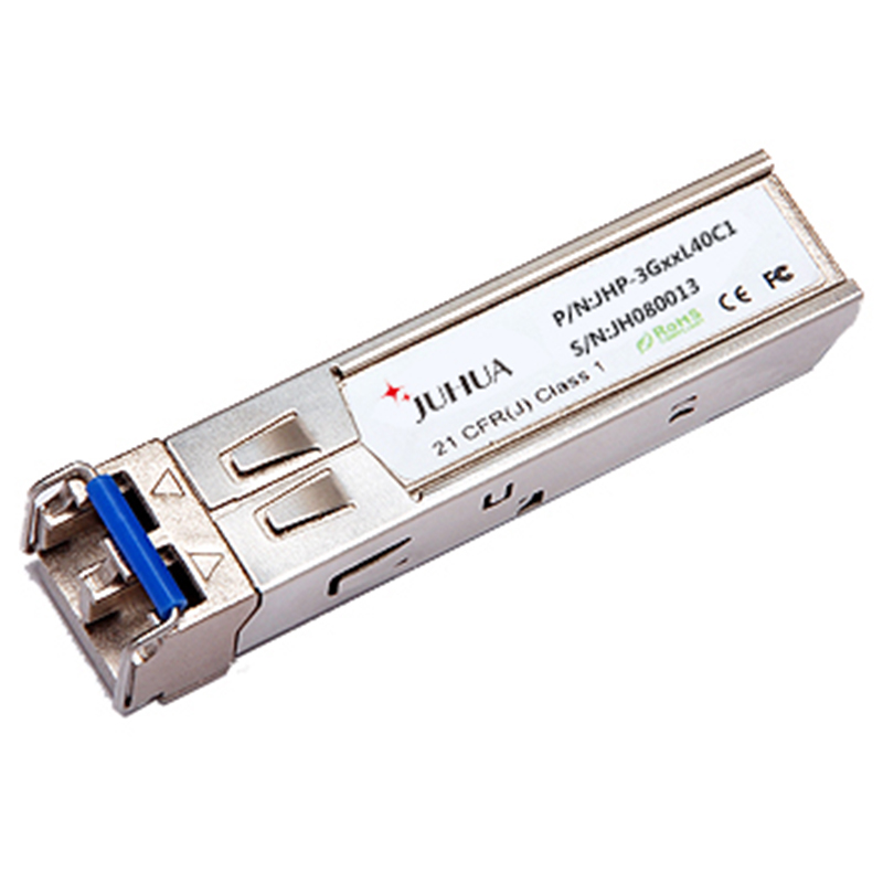
JHP-3GxxL40C1 | CWDM, 3Gbps, 40km, 0oC ~ +70oC, With Digital Diagnostic Monitoring |
Important Notice
Performance figures, data and any illustrative material provided in this data sheet are typical and must be
specifically confirmed in writing by JUHUA before they become applicable to any particular order or
contract. In accordance with the JUHUA policy of continuous improvement specifications may change
without notice.
The publication of information in this data sheet does not imply freedom from patent or other protective rights of JUHUA or others. Further details are available from any JUHUA sales representative.
Email: sales@juhuainc.com
http://www.juhuainc.com
Revision History
Version | Date | Description |
V0 | Mar. 10th, 2012 | New release |
V1 | Oct. 20th, 2021 | Change Max PRBS receiver sensitivity SD-SDI -25dBm, HD-SDI 23dBm,3G-SDI 18dBm to -20dBm; Change Max pathological Rx sensitivity SD-SDI -25dBm to -16dBm, HD-SDI -23dBm to -15dBm, 3G-SDI -18dBm to -14dBm |